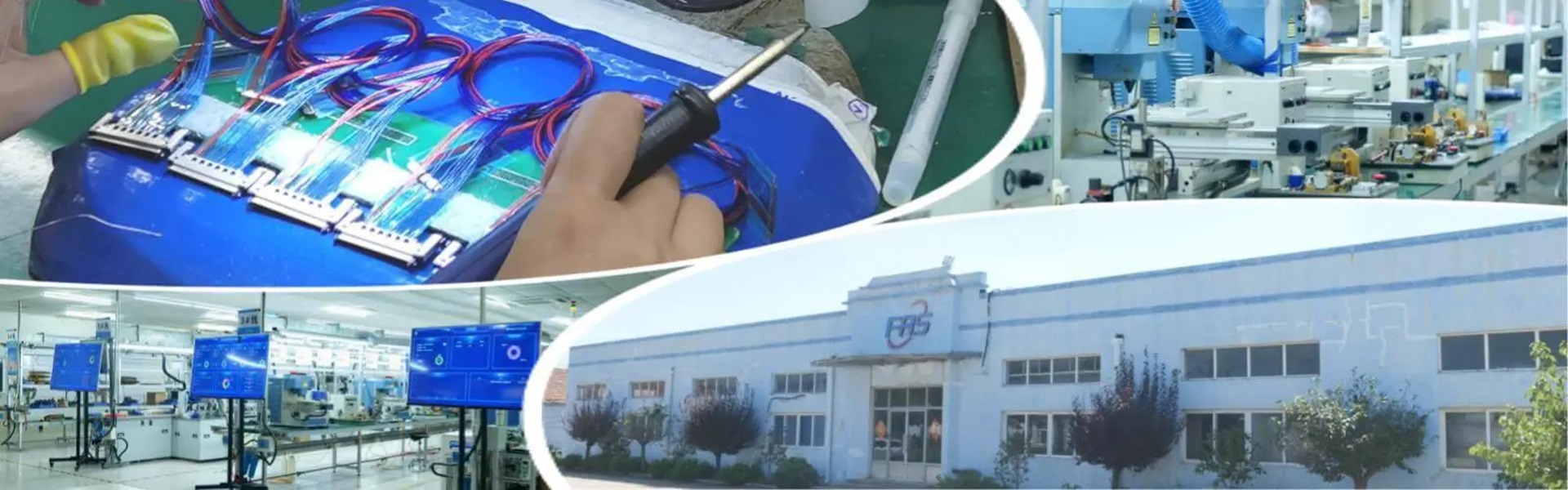
Nanotechnology in Cables: A Leap for Machine Vision Precision
- Nanomaterials Redefining Cable Architecture
Nanotechnology enables cables to transcend traditional material constraints through atomic-level engineering:
Nanomaterial Property Machine Vision Impact
Carbon Nanotubes (CNTs) 10x higher conductivity than copper Enables 200+ Gbps speeds with zero crosstalk
Graphene Layers 95% EMI shielding efficiency Eliminates noise in high-density robotic cells
Nanoparticle Dielectrics Ultra-low capacitance (0.1 pF/m) Reduces signal distortion for 16K imaging
Self-Healing Nanocoatings Autonomously repair insulation cracks Extends cable lifespan in abrasive environments
Breakthrough: Fujikura’s CNT-infused hybrid cables reduced signal loss by 78% in ASML’s EUV lithography systems, achieving 0.5 nm alignment precision.
2. Atomic-Level Signal Integrity
Nanoscale engineering eliminates analog-era limitations:
Quantum Tunneling Suppression:
Boron nitride nanotube (BNNT) insulation blocks electron leakage, maintaining signal purity across 100m runs.
Sub-Nanosecond Latency:
Silver nanowire meshes in Hirose’s “NanoSpeed” cables deliver 0.3 ns latency for real-time robotic path correction.
Adaptive Impedance Matching:
MEMS-based nano-resistors dynamically adjust impedance (±0.1Ω) to match camera and processor loads.
Case Study: Tesla’s Optimus robots achieved 99.99% weld inspection accuracy using graphene-shielded cables that neutralized EMI from 500A welding arms.
3. Defying Harsh Environments
Nano-engineered cables thrive where traditional cables fail:
Challenge Nanotech Solution Application Example
Extreme Temperatures Zirconia nanocoating (stable up to 800°C) SpaceX’s rocket engine inspection drones
Chemical Corrosion Fluoropolymer nanocapsules repel acids Battery cell manufacturing lines
Mechanical Stress Diamondoid-reinforced strands (500K bend cycles) Amazon’s Proteus warehouse robots
Innovation: Amphenol’s “NanoArmor” cables withstood 90MPa pressure in BP’s deep-sea pipeline inspection ROVs, transmitting 4K video without latency spikes.
4. Applications Driving Adoption
A. Semiconductor Manufacturing
Atomic Defect Detection:
CNT-PCIe Gen6 cables transfer 20 TB/hour of 16K wafer images to edge AI clusters.
Yield Impact: TSMC reported a 22% yield increase after switching to nano-dielectric cables in 3nm chip production.
B. Autonomous Vehicles
LiDAR-Precision:
Silver nanowire FPD-Link III cables synchronize 48-beam LiDARs with <0.01° angular error.
Case Study: Waymo’s 5th-gen Driver saw a 35% drop in false positives after adopting EMI-immune nanocables.
C. Medical Imaging
Microscopic Imaging:
Graphene-coaxial cables enable 10K endoscopes to stream 120 fps video with zero motion blur.
Breakthrough: Olympus’s nano-enhanced endoscopes detected 500µm precancerous lesions undetectable by traditional systems.
5. Overcoming Nanotech Adoption Barriers
Challenge Solution Progress
High Production Cost Roll-to-roll CNT synthesis ($0.01/cm by 2028) LG Chem’s pilot plant achieves 90% cost reduction
Standardization IEEE P2851 “NanoCable” protocol (2025 draft) Supported by Intel, NVIDIA, and Basler
Durability Concerns In-situ nanocoatings via aerosol deposition 3M’s NanoShield extends lifespan by 10x
ROI: A Bosch factory cut cable-related downtime costs by $2.1M/year after retrofitting nano-cables in its assembly robots.
6. The Future: From Nano-Engineered to Quantum-Ready
By 2035, nanotechnology will converge with quantum computing and AI:
Quantum Key Distribution (QKD) Cables:
Diamond NV centers in fibers enable hack-proof vision data transfer.
Self-Optimizing Nano-Mesh:
Cables restructure conductor paths in real-time to avoid damaged sections.
Energy Harvesting:
Piezoelectric nanowires convert robotic vibrations into power for edge sensors.
Vision: DARPA’s “Bio-Nano” project aims to grow cables with DNA-guided CNT self-assembly, reducing human manufacturing steps by 90%.